This product has been designed to simplify the implementation of TFT
technology into your product. The high level text based object oriented
command structure, entity library and 100 page screen memory allow most of
the processing to be undertaken by the TFT module leaving the host CPU to
concentrate on the core application processes. This allows proven firmware
running on small 8 bit microcontrollers to be modified to drive
this TFT module
with a minimum of work and risk.
|
|
Optical & Environmental Parameters |
|
Screen Type |
320x240 pixels - RGB Stripe - Pixel Pitch 0.22x0.22mm |
|
Display Area |
70x53mm - 3.5"
diagonal |
|
RGB
Colours |
262,144 (18
bit) |
|
Display Type |
Transmissive |
|
Contrast Ratio |
250:1 |
|
View Angle (typ) |
60 degrees |
|
Response Time |
25ms @ 25C |
|
Default Viewing
Angle |
6 o'clock (12
o'clock-Invert the PCB and set 180 degrees orientation in software) |
|
Operating
Temperature |
-20C to +70C |
|
Storage
Temperature |
-30C to +80C |
|
Humidity |
20% to 70% RH |
|
Vibration
|
10-55-10Hz, all amplitude
1mm, 30Min., X-Y-Z (Non operating) |
|
Shock |
392m/s2 (40G)
9mS X-Y-Z, 3 times each direction (Non operating) |
|
|
Electrical Parameters |
|
Parameter |
Sym |
Min |
Typ |
Max |
Unit |
Condition |
Note |
|
Supply Voltage |
VCC |
4.5 |
5 |
5.5 |
VDC |
VSS=0V |
Absolute Max 6.0VDC |
|
Logic Supply Output |
VDD |
3.2 |
3.3 |
3.4 |
VDC |
VCC=5V |
Max50mA |
|
Logic Input Voltage |
"H" |
VIH |
-0.5 |
- |
3.4 (1) |
VDC |
VCC=5V |
/RES, K0-K24, SCK, /SS, HB, SIN, SCL,SDA |
|
"L" |
VIL |
VSS |
- |
VSS+0.5 |
VDC |
VSS=0V |
|
Logic Output Voltage |
"H" |
VOH |
3.0 |
- |
3.4 |
VDC |
IOH=2mA
VCC=5v |
K0-K24, SDA, SCL, SOUT, MB |
|
"L" |
VOL |
0 |
- |
0.7 |
VDC |
IOL=-2mA
VCC=5V |
|
"H" Level Logic Input
Current |
IIH |
- |
- |
1.0 |
uADC |
VCC=5.5V |
/RES, K0-K24, SCK, /SS, SIN, SCL, SDA |
|
"L" Level Logic Input
Current |
IIL |
- |
- |
1.0 |
uADC |
VCC=5.5V |
|
RS232 Input Voltage |
"H" |
VIH |
2 |
- |
15 |
VDC |
VCC=5V |
RXD, CTS, DSR |
|
"L" |
VIL |
-15 |
- |
VSS+0.5 |
VDC |
VCC=5V |
|
RS232 Output Voltage |
"H" |
VOH |
4 |
7 |
- |
VDC |
3kΩ to GND
VCC=5V
|
TXD, DTR, RTS |
|
"L" |
VOL |
- |
-3 |
-2 |
VDC |
3kΩ to GND
VCC=5V |
|
Power Supply Current
1 |
ICC1 |
220 |
260 |
270 |
mADC |
VCC=5V |
All dots on |
|
Power Supply Current
2 |
ICC2 |
120 |
140 |
170 |
mADC |
VCC=5V |
LED Backlight Off |
|
Power Supply Current
3 |
ICC3 |
50 |
29 |
70 |
mADC |
VCC=5V |
Reset LOW |
|
Note
(1) The voltage applied to logic signals must not exceed the rising VCC at
power on as this could affect module initialisation |
|
|
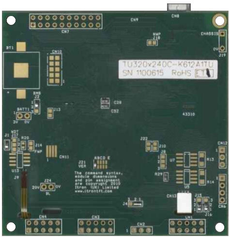
Connector
Pin Assignment
|
|
CON |
Function |
1 |
2 |
3 |
4 |
5 |
6 |
7 |
8 |
9 |
10 |
Note |
|
CN1 |
RS232 Port |
NC |
DTR |
TXD |
CTS |
RXD |
RTS |
DSR |
NC |
GND |
5V |
Fits 9 way IDC D type pin 1-9 |
|
RS232+RS485 |
T+ |
R- |
TXD |
CTS |
RXD |
RTS |
R+ |
T- |
GND |
5V |
Available on -K611xxx |
|
CN2 |
5V Power In / Piezo to GND |
5V |
/PZ |
0V |
- |
- |
- |
- |
- |
- |
- |
Connect piezo negative |
|
CN3 |
I2C Serial Mode |
5V |
SCL |
- |
SDA |
0V |
- |
- |
/RES |
|
|
3v3 Logic (5v in option) |
|
Asynchronous Serial Mode |
5V |
- |
SI |
- |
0V |
- |
SO |
/RES |
MB |
HB |
3v3 Logic (5v in option) |
|
Clock Serial / SPI Mode |
5V |
SCK |
/SS |
MOSI |
0V |
MISO |
/IRQ |
/RES |
MB |
HB |
/IRQ flags read request to host |
|
CN4 |
Analogue In, PWM Audio |
AN1 |
AN2 |
0V |
5V |
PW1 |
PW2 |
ATX |
ARX |
ACK |
AFS |
AC97 Audio Pins 7-10 |
|
User I/O |
K16 |
K17 |
0V |
5V |
K18 |
K19 |
K20 |
K21 |
K22 |
K23 |
Additional I/O |
|
|
|
|
|
|
|
|
|
|
|
|
|
|
|
CON |
Function |
1/2 |
3/4 |
5/6 |
7/8 |
9/10 |
11/12 |
13/14 |
15/16 |
17/18 |
19/20 |
Note |
|
CN7 |
8x8 Keyboard Matrix and user I/O Ports |
5V |
3V3 |
K0 |
K2 |
K4 |
K6 |
K8 |
K10 |
K12 |
K14 |
3V3 output max 50mA |
|
0V |
0V |
K1 |
K3 |
K5 |
K7 |
K9 |
K11 |
K13 |
K15 |
|
|
|
|
|
|
|
|
|
|
|
|
|
|
|
CN8 |
USB Connector |
Standard Mini B can be omitted on user
request. 5V power is then provided from the PC |
|
CN9 |
SD Card Slot |
Micro SD Card slot allows permanent
installation for large storage |
5V pins are common
un-fused input /outputs. 3V3 pins are outputs only with a total 50mA capacity. Do not
connect pins '-' or NC
|
Jumper and
Additional Connector Information |
|
JMP/CON |
Function |
Note |
|
BT1 |
Battery Connector |
Apply solder bump to center pad before fitting
holder. CR1216 battery positive up. |
|
BATT1 |
RTC alternate power 3VDC |
Apply right angle connector top side soldered. |
|
BL |
LED Backlight alternate supply |
When the backlight is software disabled, 30VDC
at 20mA can be applied by the user. |
|
J4 |
RTS Jumper |
Solder 1 and 2 for RTS. |
|
J15 |
RTS+RS4/DTR Jumper |
Solder 1 and 2 for RTS and RS485 if fitted,
solder 2 and 3 for DTR when RS485 not fitted. |
|
J16 |
CTS+RS4/DSR Jumper |
Solder 1 and 2 for CTS and RS485 if fitted,
solder 2 and 3 for DSR when RS485 not fitted. |
|
xWP |
Write protect jumpers |
Solder to prevent data update of non volatile
memory where fitted.N=Nand, EE=EEPROM. |
Note: RTS/CTS or DTR/DSR can be selected, not both. When RS485 fitted in
model K611A1xx then only RTS/CTS are possible.
|
|
